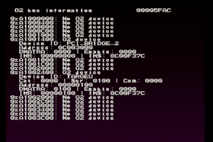
First message from G2 device
About a week or two after the previous entry, I decided to take a stab at getting started with the G2 device which I’m tentatively calling the Dreamcast Data+Network Adapter. To get the signals, I designed a set of PCBs to allow for a logic analyser to be attached during a known good device’s operation. In this case, it’s the Broadband Adapter.
Still being relatively new to HDL, I am making the mistake that a lot of software developers probably do when starting out with any HDL project. Treating it like software. There’s a lot still to learn and I don’t think that I have a good grasp on the timing issues yet. Initially, I wanted to run the FPGA at 100MHz and use the built-in PLLs to create that clock from the G2’s 25MHz bus. It seems as though there are timing issues that I don’t understand and had to drop it to 50MHz. Maybe I’ll figure out the problem with the PLL (if there is one) and get it back to 100MHz. 50MHz may be enough for at least the BBA and SD card side of things. The modem could be a different story. It doesn’t have to do any real processing at 56MHz like the MDP on an original Dreamcast unit so it should be okay.
The bus is like a reduced PCI bus. There are 32 signals, 16 for the AD, two for the BE, two for MIDI I/O, FR, TR, ST, DS, three IRQ lines, IR for the modem and external device, a CS for the modem, reset, and clock.
Here are the results after a week of hardware design:
Not quite working, but getting most of the signal correct:
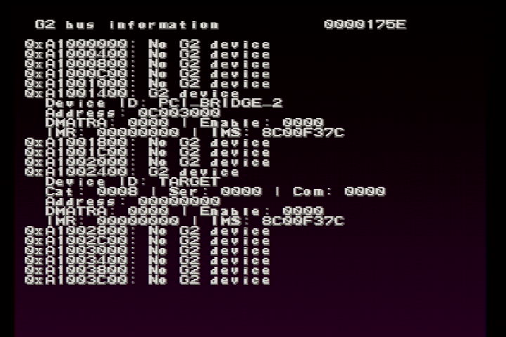
After adjusting the TR and DS drivers, it works as exepected:
Next up are the one- and two-byte reads as well as writes for all three. After that, DMA to and from the device. The SD card will probably be the least difficult of the three devices to implement. Currently, I’m thinking of supporting up to 32GB SD cards, though I’m not sure of the file system. ext2 and FAT32 would be more period-correct, but there’s nothing stopping a different sile system from being used. I’m guessing the modem (and the modem-to-LAN) will be the most challenging aspect alongside reducing the used logic cells to go below the current 84K LUT FPGA.
I’ll clean up the KiCAD files and will upload them here.