Some G2 bus details
I haven’t made time to explore the G2 bus further. I have, however, been busy working on the FPGA side of things, reading specifications for days-on-end, and figuring out a more flexible content pipeline for the Dreamcast game.
The least I can do is provide some documentation here for what I’ve leant about the G2 bus. Due to the sixteen channels available on the logic analyser I’m using, some assumptions are made on the bits of AD that can’t be read at the same time as the rest of the signals. Also, documentation is outside my usual day-to-day work, so this post may evolve over time. I’m tempted to use LaTeX for this instead, but I digress.
The connector
The G2 connector consists of 50 pins. There are two part numbers, both from AMP (now under TE Connectivity) designated as 212-5708 (host/receptacle) and 212-5709 (target/plug). These are a part of the CHAMP docking connector line, though it seems to have been fabricated specifically for the Dreamcast.
Below is the pin assignment for the connector. Names ending with ‘#’ are active-low logic.
| Pin(s) | Name | Notes |
|---|---|---|
| 1-4 | 5V | Power |
| 17-19 | 3V | Power |
| 10-12, 23, 24, 41, 42, 44, 45, 47, 48 | GND | Ground |
| 5 | MDMCS# | Modem chip select |
| 6 | IRMDM# | Modem interrupt |
| 7 | RQDEV# | Request for development device |
| 8 | RQEX1# | Request for external device 0 |
| 9 | RQEX0# | Request for external device 1 |
| 13 | IREXT# | Interrupt request for external device |
| 14 | BL# | Byte low |
| 15 | ST# | Stop |
| 16 | BH# | Byte high |
| 20 | DS# | Device select |
| 21 | FR# | Frame ready |
| 22 | TR# | Transmit ready |
| 25-40 | AD[15:0] | Address/Data |
| 43 | CLK | Bus clock |
| 46 | G_RST | Reset |
| 49 | MIDIIN | MIDI input |
| 50 | MIDIOUT | MIDI output |
The Hardware
There will be many grizzled and greenhorn KiCad users alike who could do a much better job of creating the following footprints, schematics, and PCBs than I. However, it has so far worked for me. There are two components: the connector footprint and the PCBs. The footprints may need to be added to one’s library before proceeding, though I didn’t experience an issue when trying this on a new machine. The font used (Signika) was not installed and didn’t make a difference to being able to open the file.
Here are the files:
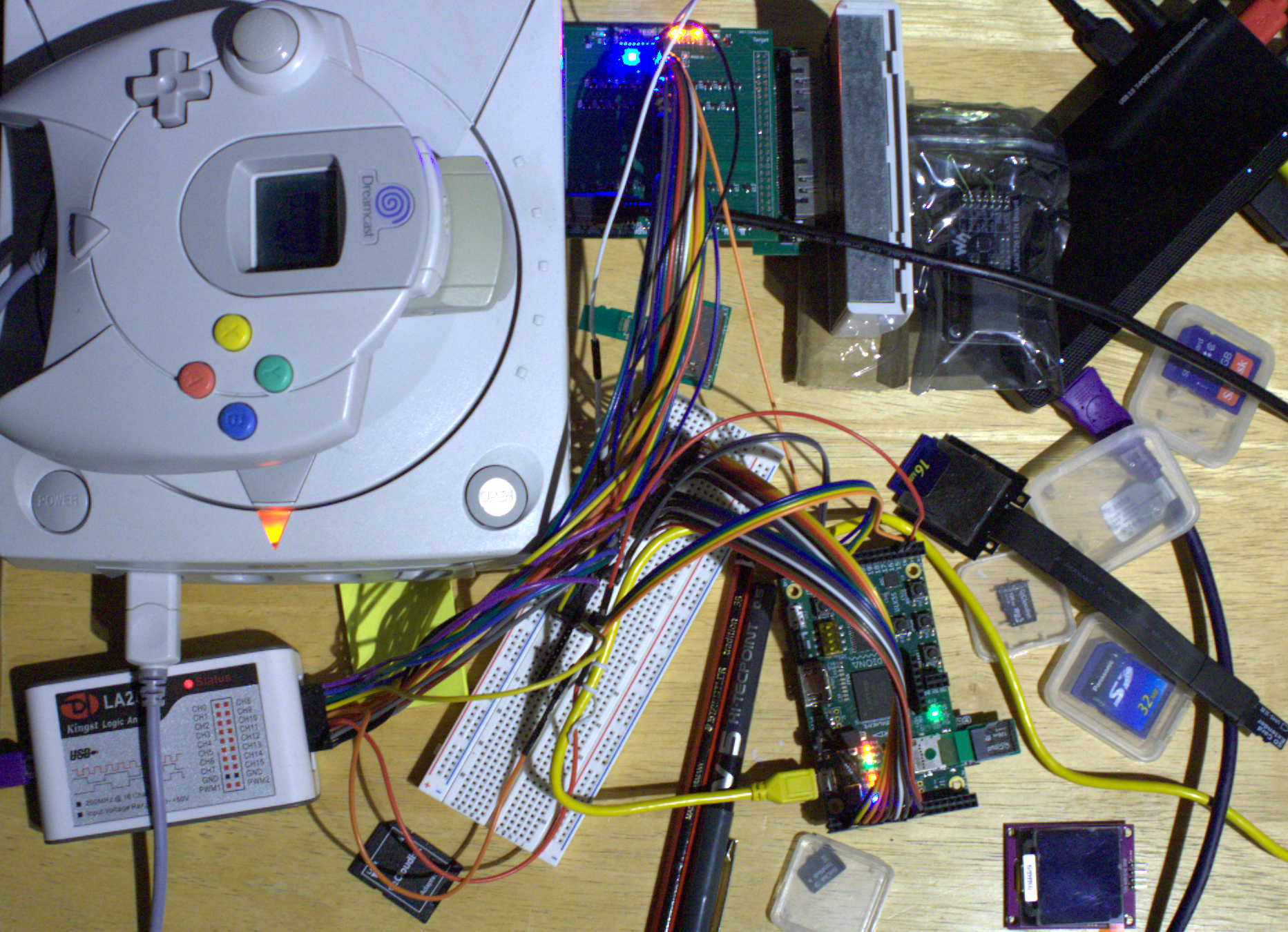
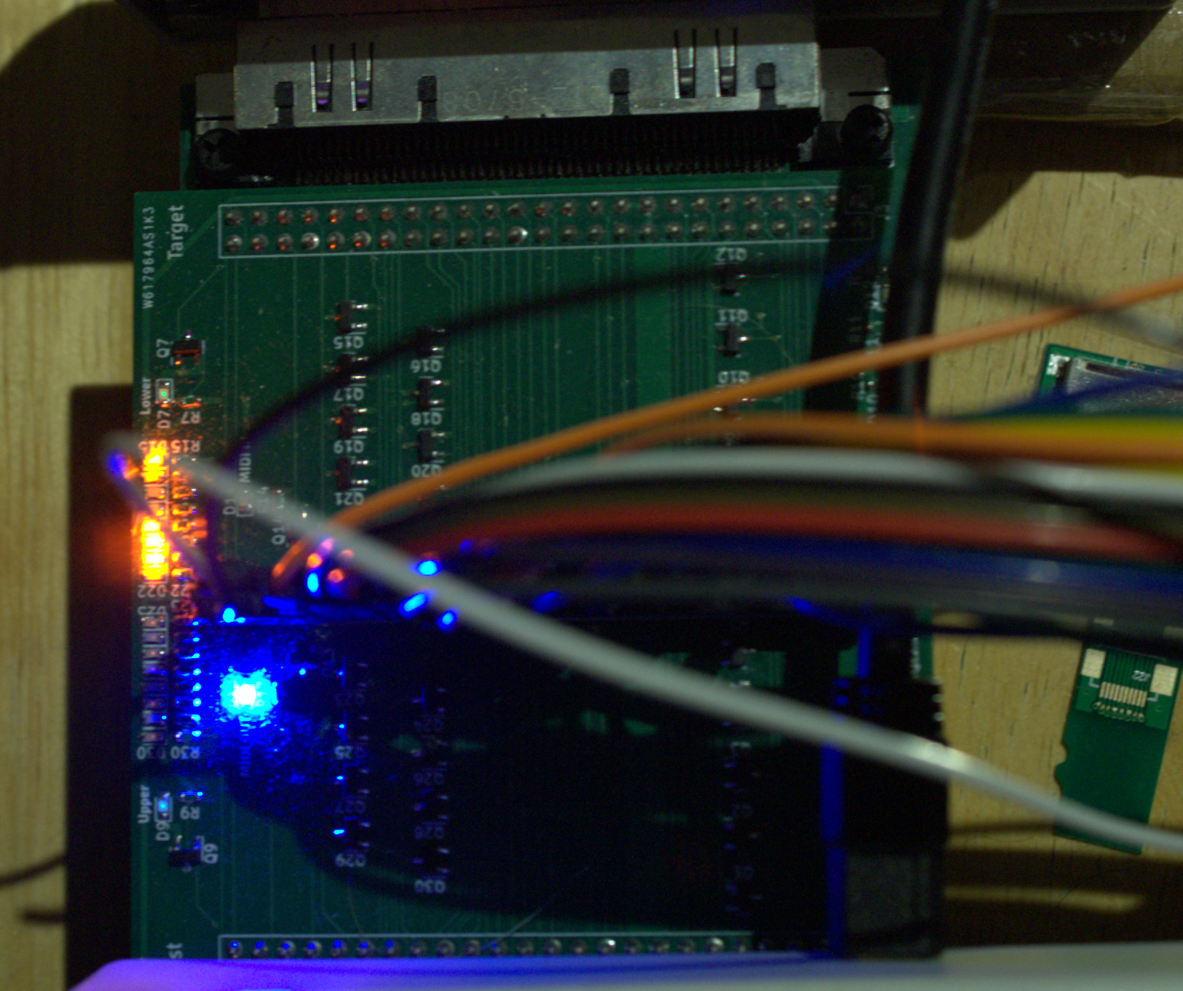
This is what it looks like in all its glory (sorry for the logic analyser in the way, I didn’t want to disturb the existing setup). It shows the debug bridge (hence all the lights), and the host and target adapters. In order to get the host adapter, a parts Dreamcast was used. I’m still looking for a good method to fabricate the connectors so that no Dreamcasts (or their modems) need to be harvested from other units.
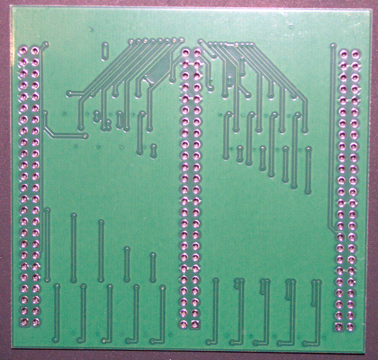
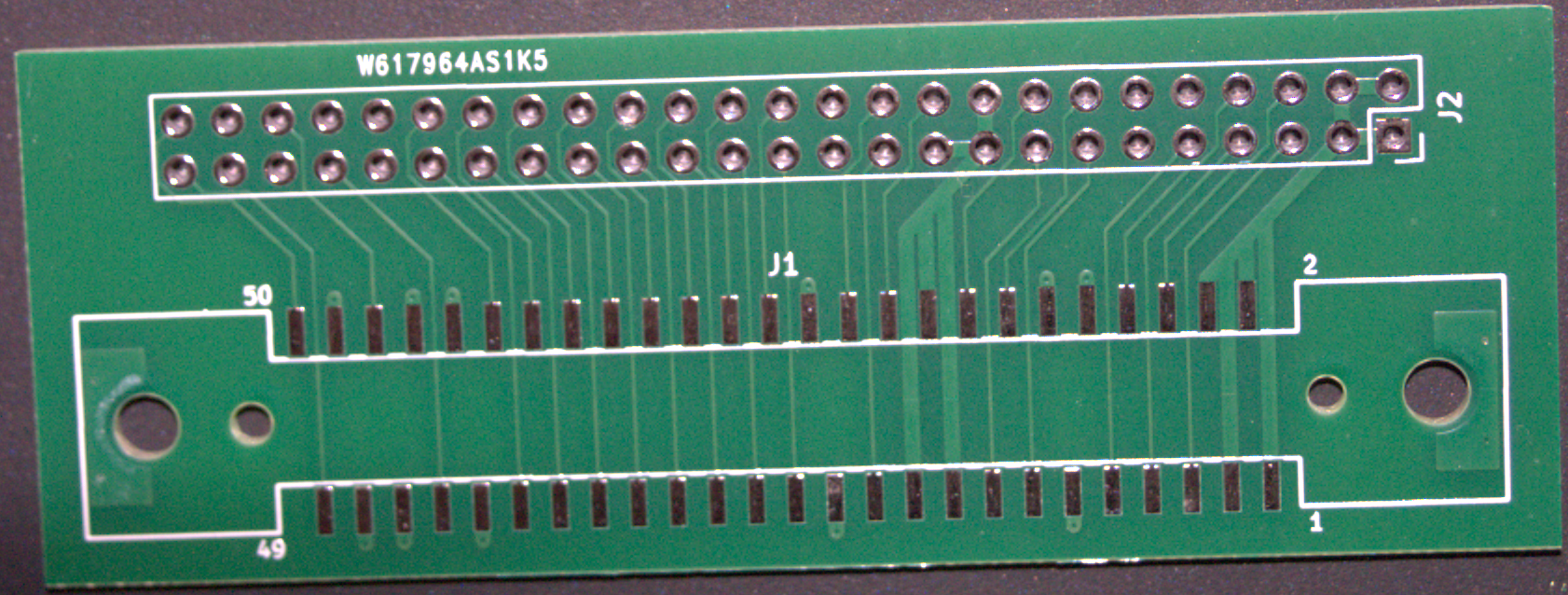
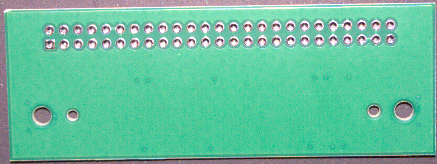
These are the individual unpopulated PCBs (open the images to view them in their original size):
Bridge
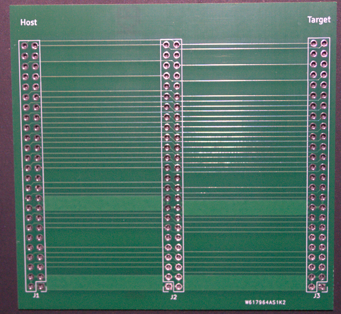
Debug bridge
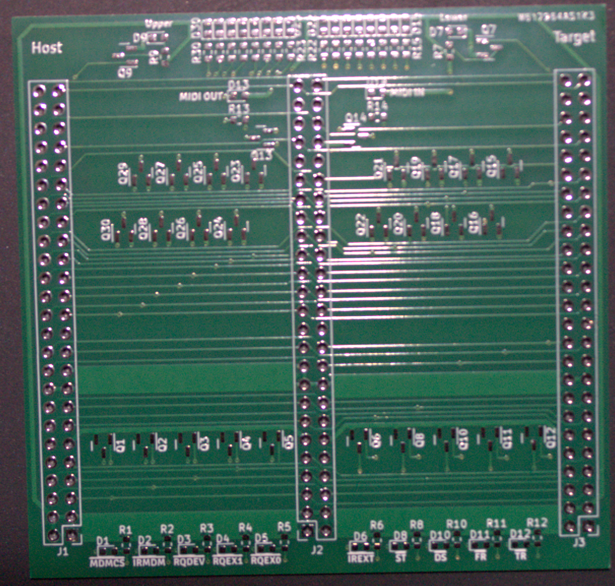
Host extender


Target extender
The signals
This is where the speculation begins. Until all signals can be captured, I’m not going to detail the DMA (this will be done within Q1) and the higher bits of AD are assumed as what should be present. I’ve uploaded the logic analyser capture from Kingst, along with the signal names. As far as I can tell, anyone may use this software. I’ve written a plugin for it to decode the Maple bus and intend to do the same for the G2 bus once I’m able to get a 32 channel logic analyser.
Here are the files: Signals and names
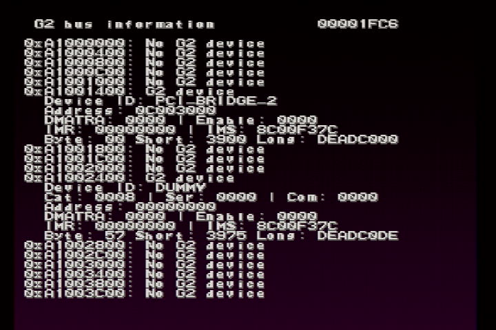
The test that ran consisted of reading the G2 information into a buffer 32 bytes wide (8 4-byte reads), followed by a series of writes which were each read as they were issued to confirm the data was present. The write and read were for 1-, 2-, and 4-byte values of 0x57, 0x3975, and 0xDEADC0DE.
As can be seen from the screenshot taken, the Broadband Adapter doesn’t seem to write the last short. This may either be a quirk of the adapter, intended behaviour, or the adapter needs to be initialised before the last short can be written.
Also, only the signals involved are captured. This consists of the high byte, low byte, frame ready, transmit ready, device select, and AD[10:0]. CLK is 25MHz, which should be taken into consideration with this 50MHz capture. There are 16 calls to devices attached to the G2 bus, plus the AICA at the start. It should become apparent where the start and end of the G2 calls takes place due to the 60Hz update rate.
Transactions
A transaction starts with a request from the host (Dreamcast) to the target by asserting FR# low. It is held low until the last transaction is read (only 4-byte transfers will hold it longer).
To indicate a read or write operation, during FR# going low, BH# must be high, with BL# indicating the direction (high = read, low = write). BL# and BH# may be performing the same role as C/BE# in PCI.
The lower part of the address (bits 15:0) is sent first. When BL# and BH# are asserted low, this indicates the high part of the address (bits 31:16). After the high part, a wait state is inserted by the target, following which, the host waits for TR# to be asserted low by the target, this indicates that the data is ready. DS# is held low by the target as long as the transaction is taking place. It is released when the last TR# is indicated.
AH indicates the upper 16 bits of an address
AL indicates thw lower 16 bits of an address
B indicates a byte (8 bits - AD[0:7])
W indicates a word (16 bits)
LH indicates the upper 16 bits of 32-bit data
LL indicates the lower 16 bits of 32-bit data
Byte
To indicate a byte transfer, BL# is asserted low and BH# is high after the address is sent. BH# remains high for the rest of the transfer process.
Read
Write
Short
To indicate a short transfer, both BL# and BH# are asserted low after the address is sent.
Read
Write
Long
To indicate a long transfer, both BL# and BH# are asserted low after the address is sent. Two TR#s are used to complete the transfer, with the host setting FR# high after the first transfer completes. A wait state seems to be used by the target after the first transfer.
Read
Write
Outro
I hope this has been useful to anyone who is considering creating peripherals for the G2 bus. I’ll still be working away on the Data and Network Adapter to support Flash cards as well as Ethernet and PPP networking. With any luck, the Flash card and Ethernet will have made some great strides by the end of the year.